报告人:陈伟 教授 (新加坡国立大学)
邀请人:苏陈良 教授
时间:2023年11月15日下午16:30
地点:深圳大学沧海校区致腾楼223会议室
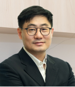
报告人简介:
Professor CHEN Wei is currently a Full professor in both the Chemistry Department and Physics Department at the National University of Singapore (NUS). He received his Bachelor degree in Chemistry from Nanjing University (China) in 2001 and his PhD degree from the Chemistry Department at NUS in 2004. His current research interests include molecular-scale interface engineering for 2D materials based electronics and optoelectronics, and interface-controlled nanocatalysis for energy and environmental research.
报告摘要:
Two-dimensional (2D) layered materials like graphene and transition metal dichalcogenides (TMDs) have been considered as promising building blocks for the next generation nanoelectronic devices, showing great potentials to extend the scaling limits existing in silicon based complementary metal-oxide-semiconductor field-effect-transistors (CMOS-FET) as well as to serve as a high mobility alternative to organic semiconductors for flexible electronic and optoelectronic devices. However, the existence of large contact resistance at the interface between the TMDs semiconductor and any bulk (or 3D) metal drastically restrains the intrinsic transport properties of materials and the performance of realistic devices. Thus, it is a crucial to optimize the contacts and lower the contact resistance between 2D semiconductors and metal electrodes.
In this talk, I will summarize and discuss our recent work for the development of scalable Ohmic contact engineering approaches to 2D materials that can be easily integrated into existing semiconductor device production processes. We will focus on the Ohmic contact to 2D materials enabled by surface charge transfer doping induced semiconductor-to-metal phase transition, and the demonstration of high performance 2D materials based electronic devices with Ohmic contact.
欢迎各位老师和同学参加!